3 January 2000
Source: Fax of 26 pages from Anonymous.
VERSION 1.0
August 1, 1996
NTT Electronics Technology Corporation
This document contains information on a product under development. NTT
Electronics Technology reserves the right to change or discontinue the product
without notice.
1. GENERAL INFORMATION2.1 Processor operation
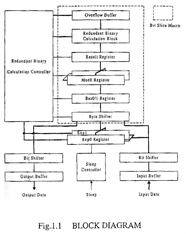
2.2 Block diagram
4.1 Register Table
4.2 Register Description
4.2.1 Status0 Register
4.2.2 Status1 Register
4.2.3 Command Register
4.3.4 Data Register6.1 Operation example using Exp0, Mod0, Bas0
6.2 Operation example using Exp1, Mod1, Bas1
7.1 Maximum ratings
7.2 Guaranteed Operating Ratings
7.3 DC Characteristics
7.4 AC Characteristics
8.1 PIN Assignments
8.2 Package Dimensions
This short form data sheet provides general information on the design and
functionality of the single chip Modular Exponentiation Processor (NLC0048).
This LSI can perform the high-speed modular exponentiation processing required
in RSA public key cryptography and Diffie-Hellman key distribution systems.
|M|, |n|: the bit length of M, n respectively
The arithmetical operations of the RSA algorithm are multiplication and division involving integers that are hundreds of digits long. The redundancy binary representation method reduces carry propagation delay and makes the operation exceedingly fast. In the conventional method, however, the most significant bit of the divisor must always be '1' to solve the quotient. This means only certain bit-length keys are available. In order to solve this problem, if the bit length of the divisor is less than 1024, it is automatically multiplied so that it becomes 1024, and the message to be operated is also multiplied by the same multiple. Then the operational result to be read out is divided by the same multiple at the output stage. The operational flow is as follows:
(1) The exponent parameter is written in the Exp0 or Exp1 register from the most significant byte. The first byte of all 'o' is discarded automatically. If the exponent is already written, this operation is unnecessary.(2) The modulus parameter is written in the Mod0 or Mod1 register from the most significant byte. The input controller multiplies 2k so that the bit length of the modulus parameter becomes 1024. The input data is multiplied by 2k in the LSI.
(3) The start command triggers the operation. The calculation is perfomred in the iterative bit slice macro. The round number depends on the bit length of the exponent in Exp0 or Exp1.
(4) The result data is divided by 2k, and a byte is attached to the first byte to be read out which indicates the effective byte length of the result data. The data sent out from the most significant byte.
(1) Input Buffer / Bit Buffer
Input data is sequentially induced to the input buffer by 8 bits. When writing in the Mod0/1 register, the position of the most significant '1' in the input stream is searched for, and a new 8 bit byte is configured so that the most significant bit of the byte becomes '1'. Then the new byte is transmitted to the Byte Shifter. The shift count in the Input Bit Shifter is memorized in the shift counter and the total effective byte length of the modulus data is calculated in this procedure. The input data to be operated, which will finally be written in the Bas0/1 register, is also shifted by the same count as the modulus data shifted in the Input Bit Shifter.The exponent data to be written in Exp0/Exp1 is transmitted transparently to each register.
(2) Output Buffer / Bit Shifter
When reading from the Result and Mod0/1 register, the 'o' bits, whose number was saved in the shift counter in the Input Bit Shifter, are fulfilled at the upper part of the first byte to be read out. If all bits in the first byte to be read out become 'o', this byte is discarded and the next byte is checked. The total effective byte length, which is calculated from the effective byte length of the modulus data and the discarded bytes in the Output Bit Shifter, is attached to the first byte of the output data.
When reading from the Exp0/Exp1 register, the effective byte length is also attached to the first byte of the read out data, which is memorized in each register at the writing stage.
(3) Byte Shifter
The input data arranged at the Input Bit Shifter is induced to the Byte Shifter except in the case of Exp0/12 writing. When writing is completed, all bytes in the Byte Shifter are shifted so that the most significant byte is not vacant. When register reading except for Exp0/1, the output data is latched in this Byte Shifter, and transmitted to the Output Bit Shifter by 8 bits.
(4) Exp0/Exp1 Register
Exponent data are stored in each register with their effective byte length. The contents of Exp0 and its byte length can be held without a power supply by the backup battery.
(5) Bas0/Bas1 Register
The registers which hold the data to be operated.
(6) Mod0/Mod1 Register
The registers which hold the modulus data.
(7) Result Register
The register which holds the intermediate data during operation and finally holds the result.
(8) Redundant Binary Calculation Block
The modulus exponentiation operation is carried out in this block. The multiplication or division of 1024 bits data is completed within one system clock.
(9) Overflow Buffer
The Overflow Buffer receives data of more than 1024 bits which results from the multiplication of two numbers both with a 1024 bit length. The contents are used at the division stage.
(10) Redundant Binary Calculation Controller
The controller which generates signals and supplies timing signals to each block of the LSI.
(11) Sleep Controller
The sleep controller stops the inner clock to reduce power consumption.
Table 3.1 Signal List (1/2)
| Signal Name | Mnemonic | I/O | Function |
| Power Supply | Vdd | - | +3.3V Power Supply |
| Ground | Vss | - | Ground Connection |
| System Clock | CLK | I | max 37MHz |
| Sleep Mode | Sleep* | I | Suppress clock to reduce power consumption. Chip is inactive when Sleep* is inserted, but can be restarted successively when Sleep* is negated. |
| Reset | Reset* | I | Used to reset register except Exp0 and its byte length register, which are used as private key register in RSA cryptograph system. Reset* must be asserted during the transition of Vdd between on and off to guarantee the information in these registers. |
| Chip Select | CS* | I | Enables input signals. |
| Write Strobe | WR* | I | Strobes the data on D7 - D0 at the trailing edge (rising edge) of WR*. |
| Read Strobe | RD* | I | Output buffer drives read out data to D7 - D0 when RD*is active. |
| Address Bus | A1 - A0 | I | Assigns registers (A0:LSB) |
| Data Bus | D7 - D0 | I/O | Bidirectional data bus of 8 bit width. |
| Error | ERROR | O | Indicates the occurrence of an operational error. |
| Operation Busy | BUSY | O | Indication that calculation is proceeding. |
| Data Wait | WAIT | O | Indicates that data writing is inhibited.
|
| Signals with * at the end of mnemonic are low active | |||
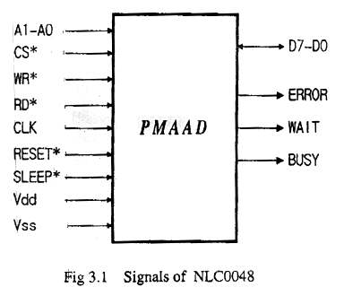
Table 4.1 Register Summary
| Register | Address | D7 | D6 | D5 | D4 | D3 | D2 | D1 | D0 |
| Status0 | 0 | Error | I/O
Ready |
Command
Ready |
Busy | Busy0 | Mod0 | Exp0 | Bas0 |
| Status1 | 1 | Error | I/O
Ready |
Command
Ready |
Busy | Busy1 | Mod1 | Exp1 | Bas1 |
| Command | 2 | Reset | Abort | Start | 0/1 | W/R* | Register | Register | Register |
| Data | 3 | MSB | LSB |
Status0/Status1: Read Only Register Command/Data: Read-Write Register
D1 bit in Status0 is always '1', and D4 bit in Command Register is unused.
Data register is not a real one but is a general name of the Result, Mod0/1, Exp0/1 and Bas0/1 registers.
4.2.1 Status0 Register
LSI status is observed from this register when calculation is performed with
Exp0, Mod0 and Bas0.
(1) Error
Next operation will cause Error to turn on.(a) Read/write option in Data Register is performed when I/O ready bit is "low".(b) Write operation is carried out when command bit is "low".
(2) I/O Ready
Before writing data in the Mod0, Exp0 and Bas0 registers, the register to be accessed and the write/read operation must be designated by writing both Register and W/R* field in the Command register. The registers are accessible when the I/O ready flag is "high". After completing the read operation from the Result, Mod0, Exp0 and Bas0 registers, the I/O ready flag switches off.
(3) Command ready
This flag indicates that the write operation in the Command register is available. The Status register must always be checked before the Command write operation. A read operation from the Command register is always possible even when the Command ready flag is "low". LSI operation is not guaranteed if command register writing is carried out when the command ready flag is off. One exception is that Abor command writing is available during an arithmetic operation.
(4) Busy
This flag indicates that an arithmetic operation is in progress. Abort command is available only when this flag is "high".
(5) Busy0
This flag indicates that an arithmetic operation is in progress using the Mod0, Exp0 and Bas0 registers.
(6) Mod0
This flag indicates that data is already written in Mod0.
(7) Exp0
This flag is always "high" because Exp0 can be held by the battery.
(8) Bas0
This flag indicates that data is already written in Bas0. If a writing operation in the Mod0 or Bas1 register is undertaken after writing in the Bas0 register, the Bas0 flag will switch off and subsequent successive operation is not guaranteed.
4.2.2 Status1 Register
LSI status is observed from this register when a calculation is performed with Exp1, Mod1 and Bas1.
(1) Error
This flag has the same meaning as Status0.
(2) I/O Ready
Before writing data in Mod1, Exp1 and Bas1 registers, the register accessed and the write/read operation must be designated by writing both Register and W/R* field in the Command register. The registers accessible when the I/O ready flag is "high". After a read operation from the Mod1, Exp1 and Bas1 registers, the I/O ready flag switches off.
(3) Command ready
This flag has the same meaning as in Status0.
(4) Busy
This flag has the same meaning as in Status0.
(5) Busy1
This flag indicates that an arithmetical operation is in progress using the Mod1, Exp1 and Bas1 registers.
(6) Mod1
This flag indicates that data is already written in Mod1.
(7) Exp1
This flag indicates that data is already written in Exp1.
(8) Bas1
This flag indicates that data is already written in Bas1. If a writing operation in the Mod1 or Bas0 register is completed after writing to Bas1 register, the Bas1 flag will switch off and subsequent successive operation is not guaranteed.
4.2.3 Command Register
(1) Reset
Writing the Command Register with "high" Reset field will initialize all the registers in the LSI except Exp0 and its byte length register. This command is always available except under Sleep mode. The reading result of the Reset filed is always "low".
(2) Abort
The Abort command stops the calculation of modular exponentiation, and makes the Result register unavailable. The simultaneous designation of both the Start and Abort commands invalidates the LSI operation. The reading result of the Abort field is always "low".
(3) Start
The Start command starts the calculation after byte shifting in the Byte Shifter. The simultaneous designation of both the Start and Abort commands invalidates the LSI operation. The reading result of the Start field is always "low".
(4) W/R*
This field designates write operation ("high") or read operation ("low") to the registers assigned by the Register field.
(5) Register
The Register field specifies the register to be accessed in the following read or write cycle.(a) Result Register (Read only)This register is assigned when the modular exponentiation is read out. The first byte is the byte length of the resulted data, and is followed by the result data stream.
Command write for reading from the Result Register is possible just after the Start command, but the actual reading operation can be performed after I/O ready switches on. The contents in the Result register are held till the next Start or Reset command.
(b) Mod1 Register (Read/Write)
This register is assigned when read or write access to Mod1 is performed. The first byte is the byte length of the contents, and is followed by data stream in Mod1.
Table 4.1 Register Table
D2 D1 D0 Register Name R, W at power off 1 1 1 Result R volatile 1 1 0 Mod1 R/W volatile 1 0 1 Mod0 R/W volatile 1 0 0 Exp1 R/W volatile 0 1 1 Exp0 W nonvolatile 0 1 0 Bas1 R/W volatile 0 0 1 Bas0 R/W volatile 0 0 0 No-op - -
(c) Mod0 Register (Read/Write)This register is assigned when read or write access to Mod0 is performed. The first byte is the byte length of the contents, and is followed by the data stream in Mod0.
(d) Exp1 Register (Read/Write)
This register is assigned when read or write access to Exp1 is performed. The first byte is the byte length of the contents, and is followed by the data stream in Exp1.
(e) Exp0 Register (Write only)
This register is assigned when write access to Exp0 is performed. Even after power off, the contents in Exp0 and its byte length can be held by the backup battery. They are also held despite the Reset command. Without the backup battery, the contents after power on is undecided.
(f) Bas1 Register (Read/Write)
This register is assigned when read or write access to Bas1 is performed. The first byte is the byte length of the contents, and followed by the data stream in Bas1. Before writing in the Bas1 register, writing in Mod1 must be completed. Mod1 or Bas0 writing after Bas1 writing invalidates the LSI operation.
(g) Bas0 Register (Read/Write)
This register is assigned when read or write access to Bas0 is performed. The first byte is the byte length of the contents, and followed by the data stream in Bas0. Before writing in the Bas0 register, writing in Mod1 must be completed. Mod1 or Bas0 writing after Bas0 writing invalidates the LSI operation.
(h) No-op
No-op is assigned when Reset, Abort and Start commands are issued.
4.2.4 Data Register
The data register is not a real one but is a general name of the Result,
Mod0/1, Exp0/1 and Bas0/1 registers. The read/write operations from/into
these registers are performed by accessing the Data register after writing
the W/R and Register field of the command register. These operations are
only possible when the I/O Ready flag in the Status Register0/1 is "high".
| now | Status name | Branch condition | to | Process in this status | Flag |
| 0 | Idle | No command Write
Command Write (Write) Command Write (Read) Command Write (Start) |
0
1 5 7 |
Idling in initial state | Command Ready |
| 1 | Data Writing | No Command Write
Command Write (Write) Command Write (Read) Command Write (Start) |
1
2 3 4 |
Data writing in Byte Shifter
(Mod0/1, Bas0/1) or Data writing in Exp0/1 |
Command Ready
I/O Ready |
| 2 | Written Data Shifting
& Next Data Write |
No Command Write (Shift incomplete)
End of shift (Byte shift counter = 127) |
2
|
Shifting Data in Byte Shifter | - |
| 3 | Written Data Shifting
& Next Data Read |
No Command Write (Shift incomplete)
End of shift (Byte shift counter = 127) |
3
|
Shifting Data in Byte Shifter | - |
| 4 | Written Data Shifting
& Next Data Calculates |
No Command Write (Shift incomplete)
End of shift (Byte shift counter = 127) |
4
|
Shifting Data in Byte Shifter | - |
| 5 | Read Data Shifting | Shift Data = all '0' (Shift incomplete
End of Shift (Read Data =/ all '0') Command Write (Write) Command Write (Read) Command Write (Start) |
5
1 5 7 |
Shifting Data in Byte Shifter | Command Ready |
| 6 | Data Reading | No command Write (Read
incomplete) End of shift (Read Data Counter = 0) Command Write (Write) Command Write (Read) Command Write (Start) |
6 0
5 7 |
Sending Data from Byte
Shifter (Mod0/1, Bas0/1, Result) or Sending data from Exp0/1 |
Command Ready I/O Ready |
| 7 | Calculating & Next Command Wait | No command Write (Calculating)
End of Calculation, Abort End of Calc. & Command Write (Write) End of Calc. & command Write (Read) Command Write (Write) Command Write (Read) |
7
8 9 |
Calculating
(Waiting for next command) |
Command ready Busy |
| 8 | Calculating & Next Data Write | No Command Write (Calculating)
End of calculation Abort |
8 1 0 |
Calculating
(next Data Write) |
Busy (only the Reset, Abort commands are acceptable) |
| 9 | Calculating & Next Data Read | No command Write (Calculating)
End of Calculation Abort |
9 5 0 |
Calculating
(next Data Read) |
Busy (only the Reset, Abort commands are acceptable) |
This chapter presents the typical usage of NLC0048, from Reset command to reading the result.
-- LSI Reset --
(1) Write Command RegisterReset field: "high"
Other fields: "low"
-- Exp0 Writing --
(2) Read Status0 Register, and Check following fields.Command Ready: "high"
Exp0: "high"
note: Exp0 field is always "high".
Other fields: "Low"
If LSI returns other values, it is something invalid.
(3) Write Command Register
W/R* field: "high" (Write)
Register field: "3h"(Exp0)
Other fields: "low"
(4) Read status0, and Check following fields.
I/O Ready: "high"
Command Ready: "high"
Exp0: "high"
note: Exp0 field is always "high".
Other fields: "low"
If LSI returns other values, it is something invalid.
(5) Write Exp0/1 data to Data register by 8 bits from most significant byte.
Note: If Exp0 is already written and held by battery, (2) - (5) steps are not necessary.
-- Mod0 Writing --
(6) Write command RegisterW/R* field: "high" (Write)
Register field: "5h"(Mod0)
Other fields: "low"
(7) Read Status0 register repeatedly till fields become following state.
I/O Ready: "low" --> "high"
Command Ready: "low" --> "high"
Exp0: "high"
Other fields: "low"
(8) Write Mod0 data to Data register by 8 bits from most significant byte.
-- Bas0 Writing --
(9) Write Command RegisterW/R field: "high" (Write)
Register field: "1h"(Bas0)
Other fields: "low"
(10) Read Status0 Register repeatedly till fields become following state.
I/O Ready: "low" --> "high"
Command Ready: "low" --> "high"
Exp0: "high"
Other fields: "low"
(11) Write message data to Data register by 8 bits from most significant byte.
-- Start Command Writing --
(12) Write Command RegisterStart field: "high"
Other fields: "low"
(13) Read Status0 Register repeatedly till fields become following state.
Error: "low"
I/O Ready: "low" --> "high"
Command Ready: "low" --> "high"
busy: "high"
busy0: "high"
Exp0; "high"
Mod0: "high"
Bas0: "high"
-- Abort command writing if necessary --
(14) Write Command RegisterAbort field: "high"
Other fields: "low"
Operation can be restarted from (1), (3), (6) or (9).
-- Read command writing --
(15) Write Command RegisterW/R* field: "high" (Write)
Register field: "7h"(Result)
Other fields: "low"
(16) Read Status0 Register repeatedly till fields become following state.
Error: "low"
I/O Ready: "low" --> "high"
Command Ready: "low" --> "high"
busy: "low"
busy0: "low"
Exp0; "high"
Mod0: "high"
Bas0: "high"
(17) Read resulted data from Data register by 8 bits.
Operation can be restarted from (1), (3), (6) or (9).
-- LSI Reset --
(1) Write Command RegisterReset field: "high"
Other fields: "low"
-- Exp1 Writing --
(2) Read Status1 Register, and Check following fields.Command Ready: "high"
Other fields: "Low"
If LSI returns other values, it is something invalid.
(3) Write Command Register
W/R* field: "high" (Write)
Register field: "4h"(Exp1)
Other fields: "low"
(4) Read status1, and Check following fields.
I/O Ready: "high"
Command Ready: "high"
Other fields: "low"
If LSI returns other values, it is something invalid.
(5) Write Exp1 data to Data register by 8 bits from most significant byte.
-- Mod1 Writing --
(6) Write command RegisterW/R* field: "high" (Write)
Register field: "6h"(Mod1)
Other fields: "low"
(7) Read Status1 register repeatedly till fields become following state.
I/O Ready: "low" --> "high"
Command Ready: "low" --> "high"
Exp0: "high"
Other fields: "low"
(8) Write Mod0 data to Data register by 8 bits from most significant byte.
-- Bas1 Writing --
(9) Write Command RegisterW/R field: "high" (Write)
Register field: "2h"(Bas1)
Other fields: "low"
(10) Read Status1 Register repeatedly till fields become following state.
I/O Ready: "low" --> "high"
Command Ready: "low" --> "high"
Exp1: "high"
Mod1: "high"
Other fields: "low"
(11) Write message data to Data register by 8 bits from most significant byte.
-- Start Command Writing --
(12) Write Command RegisterStart field: "high"
Other fields: "low"
(13) Read Status1 Register repeatedly till fields become following state.
Error: "low"
I/O Ready: "low" --> "high"
Command Ready: "low" --> "high"
busy: "high"
busy1: "high"
Exp1; "high"
Mod1: "high"
Bas1: "high"
-- Abort command writing if necessary --
(14) Write Command RegisterAbort field: "high"
Other fields: "low"
Operation can be restarted from (1), (3), (6) or (9).
-- Read command writing --
(15) Write Command RegisterW/R* field: "high" (Write)
Register field: "7h"(Result)
Other fields: "low"
(16) Read Status1 Register repeatedly till fields become following state.
Error: "low"
I/O Ready: "low" --> "high"
Command Ready: "low" --> "high"
busy: "low"
busy1: "low"
Exp1; "high"
Mod1: "high"
Bas1: "high"
(17) Read resulted data from Data register by 8 bits.
Operation can be restarted from (1), (3), (6) or (9).
| Rating | Symbol | Unit | Rating |
| Power Supply | VDD | V | -0.5~4.5 |
| Input Voltage | VIN | V | -0.5~6.5 |
| Output Voltage | VOUT | V | -0.5~5.5 |
| Characteristic | Symbol | Unit | Min | Typ | Max |
| Power Supply | VDD | V | 3.13 | 3.30 | 3.47 |
| Operating Temperature Range | Ta | C | 0 | - |
70 |
| Input HIGH Voltage | VIH | V | 2.0 | - |
5.0 |
| Input LOW Voltage | VIL | V | 0 | - |
0.8 |
| Output HIGH Voltage | IOH1 | mA | -0.4 | - |
- |
| Output LOW Voltage | IOL2 | mA | - |
- |
8 |
| Characteristic | Symbol | Unit | Min | Typ | Max | Condition |
| Input HIGH Voltage | VOH1 | V | 2.4 | - |
- |
VDD=3.13V,IOH=0.4mA |
| Input LOW Voltage | VOL1 | V | - |
- |
0.4 | VDD=3.13V,IOH=8.0mA |
| Output HIGH Voltage | IIH1 | µA | -20 | - |
20 | VDD=3.47V,V1=3.47V |
| Output LOW Voltage | IIL1 | µA | -20 | - |
20 | VDD=3.47V,V1=0V |
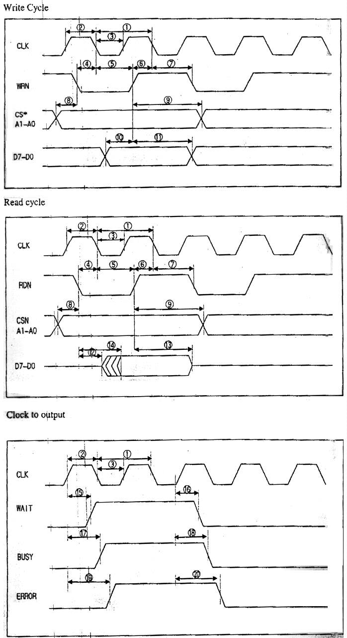
(Unit: nsec)
| Num | Characteristics | min | max |
| 1 | Clock Cycle Time | 27 | |
| 2 | Clock Pulse Width | 13.5 | |
| 3 | Clock Pulse width | 13.5 | |
| 4 | Write/Read Assert Setup Time | 10.0 | |
| 5 | Write/Read Assert Hold Time | 5.0 | |
| 6 | Write/Read Negate Setup Time | 10.0 | |
| 7 | Write/Read Negate Hold Time | 5.0 | |
| 8 | Write/Read Address Setup Time | 0.0 | |
| 9 | Write/Read Address Hold Time | 10.0 | |
| 10 | Write Data Setup Time | 5.0 | |
| 11 | Write Data Hold Time | 5.0 | |
| 12 | RD* to data-bus Driven | 25.0 | |
| 13 | RD* to data-bus Cut-off | 25.0 | |
| 14 | RD* to data-bus Valid | 30.0 | |
| 15 | CLK to WAIT Assert Time | 25.0 | |
| 16 | CLK to WAIT Negate Time | 25.0 | |
| 17 | CLK to BUSY Assert Time | 25.0 | |
| 18 | CLK to BUSY Negate Time | 25.0 | |
| 19 | CLK to ERROR Assert Time | 25.0 | |
| 20 | CLK to ERROR Negate Time | 25.0 |
note-1 Condition: External capacitance is 15pF at output pins.
note-2 The Value in 7 is required to be at least 1 tau [time constant] +5(nsec) for command write.
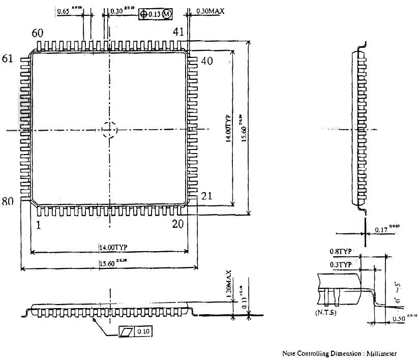
| Pin No. |
Signal Name |
I/O | Pin No. |
Signal Name |
I/O | Pin No. |
Signal Name |
I/O | Pin No. |
Signal Name |
I/O |
| 1 | Vss | POW | 21 | Vdd | POW | 41 | Vss | POW | 61 | Vss | POW |
| 2 | Vdd | POW | 22 | Vss | POW | 42 | Vdd | POW | 62 | Vdd | POW |
| 3 | #1 | O | 23 | #2 | I | 43 | A0 | I | 63 | D3 | B |
| 4 | #1 | O | 24 | #2 | I | 44 | A1 | I | 64 | D4 | B |
| 5 | #1 | O | 25 | #2 | I | 45 | Vss | POW | 65 | D5 | B |
| 6 | Vss | POW | 26 | Vss | POW | 46 | Vdd | POW | 66 | Vss | POW |
| 7 | Vdd | POW | 27 | Vdd | POW | 47 | CLK | I | 67 | Vdd | POW |
| 8 | #1 | O | 28 | #2 | I | 48 | #2 | I | 68 | D6 | B |
| 9 | #1 | O | 29 | #2 | I | 49 | Vss | POW | 69 | D7 | B |
| 10 | Vss | POW | 30 | Vss | POW | 50 | #2 | I | 70 | Vss | POW |
| 11 | #1 | O | 31 | RESET* | I | 51 | #2 | I | 71 | BUSY | O |
| 12 | #1 | O | 32 | SLEEP* | I | 52 | Vss | POW | 72 | WAIT | O |
| 13 | Vdd | POW | 33 | Vss | POW | 53 | Vdd | POW | 73 | Vdd | POW |
| 14 | Vss | POW | 34 | Vdd | POW | 54 | Vss | POW | 74 | Vss | POW |
| 15 | #1 | O | 35 | CS* | I | 55 | D0 | B | 75 | ERROR | O |
| 16 | #1 | O | 36 | WR* | I | 56 | D1 | B | 76 | #1 | O |
| 17 | #1 | O | 37 | RD* | I | 57 | D2 | B | 77 | #1 | O |
| 18 | Vss | POW | 38 | Vss | POW | 58 | Vss | POW | 78 | Vss | POW |
| 19 | Vdd | POW | 39 | Vdd | POW | 59 | Vdd | POW | 79 | Vss | POW |
| 20 | Vss | POW | 40 | Vss | POW | 60 | Vss | POW | 80 | Vdd | POW |
Signal Name
Vdd: +3.3-volt power supply
Vss: Ground connections
NC: No not connect
#1: Do not connect
#2: Do pull-up to +3.3-volt
I/O
I: Input pins.
O: Output pins.
B: Bidirectional pins.
[End]
Transcription and HTML by Cryptome.