The C.N.R. Project
The
C.N.R. Project
The Chung's Apparent Negative Resistance
Created on 05-20-01 - JLN Labs
- Last update 05-27-01
All informations in this
page are published free and are intended for private/educational
purposes and not for commercial applications
You will find bellow some interesting reflexions and ideas from the JLN Labs group-list about the CNR project :
Dans un e-mail
daté du 26/05/01 18:57:54 Paris, Madrid (heure d'été),
Tony Purser
a écrit : Hi Tony,
Willard, Christian and All, |
||||||
Hi, JL, Willard, John and all,

I have now analysed the simplified 3 * 3 Carbon Fibre model of the CNR, for the case of a non-zero
contact resistance between the crossed fibres at the nodes within the junction.
To allow for the additional height dimension, which accommodates the contact resistances,
I have had to change the notation for the nodes in the junction. I have added the prefix '0'
 to the node numbers on the A-B carbon strip, and '1' to the nodes on the C-D carbon strip.
This new notation is depicted in the diagram below, where the diagonal lines include the contact
 resistances RC. A monospaced font is probably best for viewing this diagram.

                     A             A             A
                     -----------------------------
                     :             :             :
                     :             :             :
                     :             :             :
                     :             :             :
                     :             :             :
                     :             :             :
                     :             :             :
                     :             :             :
                     :             :             :
                    011           012           013
                    /:            /:            /:
                   / :           / :           / :
                  /  :          /  :          /  :
                 /   :         /   :         /   :
                /    :        /    :        /    :
C:------------111----:------112----:------113----:-------:D
 :                   :             :             :       :
 :                   :             :             :       :
 :                  021           022           023      :
 :                  /:            /:            /:       :
 :                 / :           / :           / :       :
 :                /  :          /  :          /  :       :
 :               /   :         /   :         /   :       :
 :              /    :        /    :        /    :       :
C:------------121----:------122----:------123----:-------:D
 :                   :             :             :       :
 :                   :             :             :       :
 :                  031           032           033      :
 :                  /:            /:            /:       :
 :                 / :           / :           / :       :
 :                /  :          /  :          /  :       :
 :               /   :         /   :         /   :       :
 :              /    :        /    :        /    :       :
C:------------131----:------132----:------133----:-------:D
                     :             :             :
                     :             :             :
                     -----------------------------
                     B             B             B

The resistance of the fibre segments between the terminals and the junction is assumed to be 10 ohms,
as before.
The resistance of the fibre segments between adjacent nodes within the junction is 1 ohm, as before.
I shall use the term transfer resistance for the differential voltage VB - VD between the
voltage monitoring (output) terminals, divided by the current driven through the input
terminals A and C.
In the case of the fully compressed junction, with zero contact resistances, the transfer
resistance was previously found to be -0.276426 Ohms (a negative apparent resistance).
In the 3D model above, I solved for the value of contact resistance RC which would result
in a transfer resistance of 0 Ohms (zero apparent resistance).
This special value for contact resistance was found to be 2.51211 Ohms (contact conductance
0.398072 Siemens), for this network.
For an applied voltage at terminal A equal to 10 volts with respect to terminal C,
the following voltages (Volts) were found at the nodes of the network, at this conditon:

VA = 10.00000
VB = 5.000000
VD = 5.000000
VC = 0.000000

V011 = 5.227079          V012 = 5.475632          V013 = 5.59418
V021 = 4.930575          V022 = 5.184894          V023 = 5.308826
V031 = 4.79577           V032 = 5.04136           V033 = 5.16287

V111 = 4.772921          V112 = 5.069425          V113 = 5.20423
V121 = 4.524368          V122 = 4.815106          V123 = 4.95864
V131 = 4.40582           V132 = 4.691174          V133 = 4.83713

Once again these figures can be verified by checking that the sum of the currents into each
of the free nodes in the network is zero (Kirchhoff's Current Law). Alternatively, someone might
care to run the model on a simulator, such as MicroCap.
The reason why the apparent negative resistance, which appears for contact resistances less than
the special value of 2.51211 Ohms, cannot be used as an energy flow source, is now clear.
This apparent negative resistance is only a transfer resistance, and not a driving point resistance,
such as is provided by a standard two terminal (one-port) resistor.
For explanation of these terms, and electrical network theory in general, I used the following
text book reference:
Linear Network Analysis, by Sundaram Seshu and Norman Balabanian,
Published by John Wiley & Sons, Inc. (Third Printing 1964),
Library of Congress Catalog Card Number: 59-9352
With a bit more work, it should be possible to derive an expression for the transfer resistance
as a function of contact resistance, or at least plot a few points on the curve.

Best Regards,
Tony Purser
|
||||||
Hi, Jean, Willard, and all,
I am an Electronic Engineer, but I would not call a Tunnel Diode a negative resistor.
It is a two terminal device with a NEGATIVE SLOPE RESISTANCE over a limited range.
It may APPEAR as a negative resistance in an ac coupled circuit, if biassed at a suitable
operating point.
I would suggest some basic definitons along these lines (from the electrical circuit point of view):
IDEAL RESISTOR:
A 2 terminal device obeying Ohm's Law, and with a resistance value (in Ohms) which may be
expressed as:
V
R = ---
I
where V is the voltage (Volts) across the device, I is the current (Amperes) flowing into
the device from the more positive terminal.
The energy flow, or power (Watts) flowing into the Ideal Resistor is given by the product V * I.
IDEAL NEGATIVE RESISTOR:
An Ideal Resistor with a negative value of resistance R.
This implies that it is a net source of energy flow into the external circuit.
REAL RESISTOR:
A practical 2 terminal component which approximates the Ideal Resistor over a range of operating
conditions (voltage, current, frequency, temperature, etc.). A Real Resistor normally has a
positive value of resistance R, so is a net sink for energy flow.
REAL NEGATIVE RESISTOR:
A practical 2 terminal component which approximates the Ideal Negative Resistor over a range of
operating conditions (voltage, current, frequency, temperature, etc.). A Real Negative Resistor
should be a net source of energy flow into the external circuit. I am not aware of the existence
of any such components which are readily available or manufacturable.
APPARENT NEGATIVE RESISTOR:
A practical device which may exhibit characteristics approximating those of a Real Negative
Resistor according to a restricted definition, which may allow for a dc offset, non-linearity,
restricted frequency range, additional terminals, etc. In general, an Apparent Negative Resistor
is always a net sink of energy flow from the external circuit (taking all terminals into consideration).
A Tunnel diode with a suitable biassing and ac coupling circuit may therefore be classified as
an Apparent Negative Resistor. Of course, the dc biassing always ensures that it is a net sink of
energy flow, although this is not apparent to the ac coupled circuit.
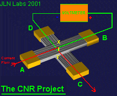
The CNR device is interesting as it appears to have almost ideal characteristics, except that it is
a 4 terminal device. This means that the pair of voltage monitoring terminals cannot be used as a
source of current into the external circuit, and the pair of current supply terminals cannot be used
as a source of voltage.
CNR
I have been thinking along the same lines as Willard, and fully agree with his conclusions. I have
not performed any tests, but have done some mathematical analysis which shows that the device must
indeed reverse its junction voltage at some stage during compression. The model of the device which
I have used for the analysis is similar to Willard's, except that I had only three fibres in each strip,
instead of four, to keep things simple. I have assumed that there is negligible conduction between
parallel fibres, as there is no compression in that direction. I have only analysed the model for
the case where the junctions are fully connected (zero contact resistance at each node in the junction
area). I assumed that each fibre tail had a resistance of 10 ohms between the junction and the
terminal, and that the resistance of each fibre between a pair of nodes is 1 ohm. This shows that
the junction voltage for the fully compressed junction is reversed with respect to the voltage
appearing across the uncompressed junction (with no internal nodes connected). This implies an
Apparent Negative Resistor for the fully compressed junction. There must therefore be some value
of contact resistance at the internal nodes, for which the device appears as zero resistance.
In the partially compressed condition, the number of nodes in the junction effectively doubles,
as there is a circuit node at each end of each contact (3D model). This almost doubles the number
of equations to solve, and I have not had time to do this so far. The results of the 2D analysis
for the fully compressed junction are given below.
The notation I used for the internal nodes of the fully compressed Carbon Fibre Junction follows
standard Matrix notation when terminal A is uppermost and terminal C is to the left:
A A A
-----------------------------
: : :
: : :
: : :
:11 :12 :13
C----------------------------------------------------------D
: : : : :
: : : : :
: :21 :22 :23 :
C----------------------------------------------------------D
: : : : :
: : : : :
: :31 :32 :33 :
C----------------------------------------------------------D
: : :
: : :
: : :
: : :
-----------------------------
B B B
I hope this is clear enough on your screen. A monospaced font may help when viewing it.
The voltages (Volts) at the terminals, relative to terminal C, are as follows:
VA = 10.00000
VB = 4.802991
VC = 0.000000
VD = 5.197009
The voltages (Volts) at the internal nodes are as follows:
V11 = 5.000000
V12 = 5.303893
V13 = 5.442069
V21 = 4.696107
V22 = 5.000000
V23 = 5.148958
V31 = 4.557931
V32 = 4.851042
V33 = 5.000000
The apparent junction voltage (Volts) is given by VB - VD:
Vj = -0.394018
The current (Amperes) flowing through the junction is as follows:
Ij = 1.425404
The apparent junction resistance (Ohms) is given by Vj / Ij, as follows:
Rj = -0.276426
This is an Apparent Negative Resistance.
Of course, in the extreme case of no nodes connected, the junction voltage Vj would be +10 Volts,
and the apparent junction resistance would be infinite (positive).
CONCLUSIONS
No exotic explanations are needed to account for the change in apparent electrical resistance from
positive to negative as pressue is applied to the juction area. If in doubt, apply Ohm's law to
calculate the currents in each branch of the above network, and verify that Kichhoff's Voltage and
Current Laws are met in each branch and node.
If this model is representative, the CNR can never become a Real Negative Resistor, as it is composed
entirely of elements with positive electrical resistance. The resistance measured in isolation across
any two terminals will always be a positive value.
The best application for the CNR may be as a strain sensor in composite structures. It has the
advantage of only requiring a voltage polarity sensing instrument to indicate a compression strain
threshold limit has been reached, and is relatively insensitve to the applied current. The large
number of carbon fibres should average out resistance variations in the individual fibres.
Tony Purser
|
||||||
Gentlemen,

Willard is fully right: the CNR mesurement are completely explained
by the old fashioned Ohm's law... I made a simulation of a 3 x 3
network with Microcap6 (no more nodes because I have an evaluation
version: 33 resistors are needed. Would be probably the same with a 2
x 2 network). I simulated the ABCD crossed network as described on
JLN site (with the same names for the connexion nodes). I used 9
resistors for the interconnexion of the two 3 x 3 layers, each has a
common value of RP=10 downto 0 Ohms. Each fiber is represented by 10
ohm resistors, connecting the 3 nodes on each side and the terminals
I apply a 10V DC source on terminal A and terminal D is grounded Basically we observe that when RP is high, V(D)< V(C), then when RP is decreased, V(D) falls down and V(C) rises (of course there is a value at wich they are equal) and then V(D)> V(C), which can be interpreted as a negative value for equivalent resistance. Actually, I became clear in my mind when I interpreted the voltages v(C) and v(D) as the output of two independant voltage dividers (potentiometers). Hope this helps to clarify , at least it showed me that old Ohm's law still hides some funny effects... Best Regards Christian Neel |
||||||
Dear JL Naudin, To clarify what happens in the CNR I did some tests. I have just created a meld of 40 resistors, simulating 4 wires resting on 4 wires in a cross hatch pattern. When I connected this to two meters as you have done I get exactly what you get for the meld is flowing the + voltage and the - voltage to the nearest adjacent terminal. The second meter with its negative terminal to the top of the meld is hooked up in reverse for a meld and so reads backwards. If you have only crossed wires or fibers lightly touching there is a high resistance in the multiple junction and the input voltage is carried through to the output on the fibers or wires and therefor the meters are connected correctly for forward reading on both input and output. Ther is no mystery. The squeezing just causes a larger surface contact area of the cylindrical shape of the crossed wires or fibers and thus a lower multipe junction resistance. This changes the crossed wires or fibers to a resistive meld. As the pressure cotinues to increase a point will be reached where the two voltages cancell befor the meld causes the voltage to reverse on the second meter. Best regards, Willard Elliott |
||||||
For
more informations, please contact : ![]() JNaudin509@aol.com
JNaudin509@aol.com
Return to the CNR home page

